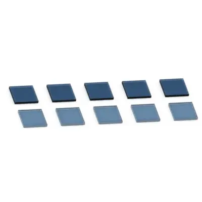
B-doped SCD 外延片 — boron-doped single-crystal diamond plate (visual identity per handbook)
B-doped SCD 外延片 — boron-doped single-crystal diamond plate (visual identity per handbook)
Diamond's 5.5 eV bandgap and 20 MV/cm breakdown field unlock power device performance impossible in silicon, SiC, or GaN. 我們的 B-doped epi wafers deliver the foundation.
20 MV/cm breakdown field — 33× silicon, 3× SiC. Enables thinner drift regions, lower on-resistance, and higher voltage operation in the same package.
在p+ SCD襯底上的工程化p−本徵漂移層。針對高壓肖特基二極管整流、p-n二極管和p溝道垂直MOSFET進行優化。
原子級表面精加工,實現直接外延生長和器件製造,無需中間拋光。標準fab兼容。
我們的 B-doped diamond epi wafers target the highest-performance power device applications — where silicon and SiC hit their physical limits.
肖特基、p-n、PiN
金剛石肖特基二極管用於電力傳輸、電動汽車牽引逆變器和併網太陽能的>10 kV整流。導通損耗低於SiC。
垂直功率晶體管
使用摻硼塊材的垂直金剛石p溝道MOSFET。目標爲電動汽車動力總成、HVDC和超高效功率轉換。
高溫、抗輻射
金剛石電子在>300°C下工作並耐受極端輻射。適用於航空航天、井下鑽探、核工業和高溫工業傳感。
我們的 SCD 外延片 (H-terminal) 使用氫端接本徵外延,用於p溝道H-金剛石FET和射頻肖特基二極管。兩種襯底變體共享金剛石外延基礎 — 不同的摻雜,不同的應用重點。
登錄 to see the standard epi wafer geometries, doping layer stacks, and surface-finish options. Custom epitaxial recipes and DFM are available for any device target.