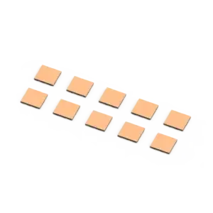
鍍銅多晶金剛石 — patterned Cu routing on PCD thermal core
鍍銅多晶金剛石 — patterned Cu routing on PCD thermal core
Cu-metallized PCD combines the thermal performance of polycrystalline diamond with the manufacturability and electrical routing of patterned copper traces.
Diamond's high thermal conductivity carries heat across the entire plate — far better than AlN or copper-only baseplates.
Patterned copper traces on the PCD surface enable electrical routing, ground planes, and bond pad arrays — all in one integrated substrate.
Copper surface enables standard SMT assembly — AuSn solder, wire bonding, and direct chip attach. Standard fab-compatible.
IGBT / SiC / GaN modules
Cu-metallized PCD baseplates for industrial power modules — combining diamond's thermal spreading with copper's electrical routing and solder attachment.
High-power laser packaging
Cu-patterned PCD submounts for high-power laser diodes. Solderable Cu traces + diamond thermal spreading = longer laser lifetime.
High-power-density baseplates
Cost-effective thermal-electrical integration for industrial electronics. Replaces AlN or direct-bond-copper (DBC) baseplates where peak performance matters.
登錄 to see the standard Cu plating thicknesses, trace geometries, and standard PCD substrate dimensions. Custom Cu patterns and DFM available.