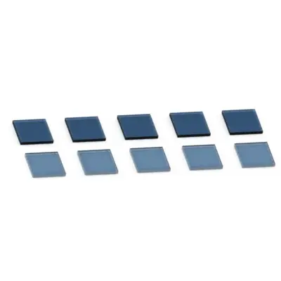
B-doped SCD Epi Wafer — boron-doped single-crystal diamond plate (visual identity per handbook)
B-doped SCD Epi Wafer — boron-doped single-crystal diamond plate (visual identity per handbook)
Diamond's 5.5 eV bandgap and 20 MV/cm breakdown field unlock power device performance impossible in silicon, SiC, or GaN. Our B-doped epi wafers deliver the foundation.
20 MV/cm breakdown field — 33× silicon, 3× SiC. Enables thinner drift regions, lower on-resistance, and higher voltage operation in the same package.
Engineered p− intrinsic drift layer on p+ SCD substrate. Optimized for high-voltage Schottky diode rectification, p-n diodes, and p-channel vertical MOSFETs.
Atomic-level surface finish enables direct epitaxial growth and device fabrication without intermediate polishing. Standard fab-compatible.
Our B-doped diamond epi wafers target the highest-performance power device applications — where silicon and SiC hit their physical limits.
Schottky, p-n, PiN
Diamond Schottky diodes for >10 kV rectification in power transmission, EV traction inverters, and grid-tie solar. Lower conduction loss than SiC.
Vertical power transistors
Vertical diamond p-channel MOSFETs using B-doped bulk. Targets EV powertrain, HVDC, and ultra-high-efficiency power conversion.
High-temperature, radiation-hard
Diamond electronics operate at >300°C and tolerate extreme radiation. For aerospace, downhole drilling, nuclear, and high-temperature industrial sensing.
Our SCD Epi Wafer (H-terminal) uses hydrogen-terminated intrinsic epi for p-channel H-diamond FETs and RF Schottky diodes. Both substrate variants share the diamond epi foundation — different doping, different application focus.
Sign in to see the standard epi wafer geometries, doping layer stacks, and surface-finish options. Custom epitaxial recipes and DFM are available for any device target.