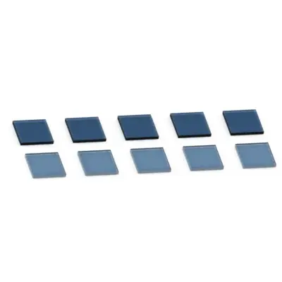
B-doped SCD 外延片 — boron-doped single-crystal diamond plate (visual identity per handbook)
B-doped SCD 外延片 — boron-doped single-crystal diamond plate (visual identity per handbook)
Diamond's 5.5 eV bandgap and 20 MV/cm breakdown field unlock power device performance impossible in silicon, SiC, or GaN. 我们的 B-doped epi wafers deliver the foundation.
20 MV/cm breakdown field — 33× silicon, 3× SiC. Enables thinner drift regions, lower on-resistance, and higher voltage operation in the same package.
在p+ SCD衬底上的工程化p−本征漂移层。针对高压肖特基二极管整流、p-n二极管和p沟道垂直MOSFET进行优化。
原子级表面精加工,实现直接外延生长和器件制造,无需中间抛光。标准fab兼容。
我们的 B-doped diamond epi wafers target the highest-performance power device applications — where silicon and SiC hit their physical limits.
肖特基、p-n、PiN
金刚石肖特基二极管用于电力传输、电动汽车牵引逆变器和并网太阳能的>10 kV整流。导通损耗低于SiC。
垂直功率晶体管
使用掺硼块材的垂直金刚石p沟道MOSFET。目标为电动汽车动力总成、HVDC和超高效功率转换。
高温、抗辐射
金刚石电子在>300°C下工作并耐受极端辐射。适用于航空航天、井下钻探、核工业和高温工业传感。
我们的 SCD 外延片 (H-terminal) 使用氢端接本征外延,用于p沟道H-金刚石FET和射频肖特基二极管。两种衬底变体共享金刚石外延基础 — 不同的掺杂,不同的应用重点。
登录 to see the standard epi wafer geometries, doping layer stacks, and surface-finish options. Custom epitaxial recipes and DFM are available for any device target.