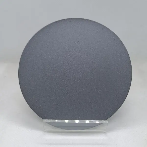
硅襯底BDD電極 — boron-doped polycrystalline diamond film on Si substrate
硅襯底BDD電極 — boron-doped polycrystalline diamond film on Si substrate
Silicon is the dominant substrate for BDD electrodes — leveraging standard semiconductor fab tooling, established supply chains, and cost-effective wafer formats.
Boron-doped diamond film (typically heavy-doped) grown directly on silicon. Combines diamond's chemical inertness with Si's standard fab compatibility.
Diamond's 5.5 eV bandgap enables a much wider electrochemical window than metal electrodes. Drives oxidation reactions that conventional materials cannot.
Diamond film is inert to acids, bases, and aggressive solvents. Operates continuously in conditions that destroy metal electrodes in days.
Industrial wastewater oxidation
BDD-on-Si electrodes for industrial water treatment — oxidizing persistent organic pollutants (POPs), pharmaceuticals, and PFAS that resist conventional treatment.
Trace analyte detection
BDD-on-Si for biomedical and environmental sensors. The wide window enables detection of analytes invisible to metal electrodes.
Wafer-level electrochemical
BDD-on-Si for semiconductor process equipment — wafer-level electrochemical etching, polishing, and surface modification.
登錄 to see the standard Si wafer sizes, BDD film thicknesses, doping tiers, and back-contact metallization options.