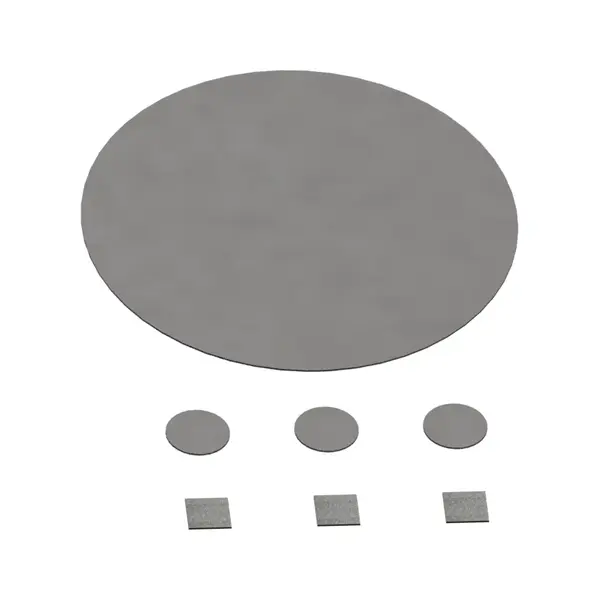
Polycrystalline CVD金刚石晶圆 — free-standing, polished surface
Polycrystalline CVD金刚石晶圆 — free-standing, polished surface
Polycrystalline diamond delivers most of the thermal and electrical benefits of SCD at a fraction of the cost — and can be grown on large-area substrates for wafer-scale applications.
PCD delivers thermal conductivity several times that of copper and silicon. Excellent for high-power thermal management at lower cost than SCD.
PCD grows on large substrates — significantly more area than SCD. Cost-effective for wafer-scale thermal and electrochemical applications.
Boron doping transforms insulating PCD into conductive material. Used as the base for our BDD electrodes on Si/Nb/Ti/glass.
PCD wafers form the substrate for our entire PCD product line — heat spreaders, BDD electrodes, and coated substrates.
GaN-on-PCD, SiC-on-PCD
PCD wafers serve as cost-effective substrates for GaN and SiC power device epitaxy. Larger area than SCD at lower cost.
Sourced for BDD electrodes on Si/Nb/Ti
重-doped PCD wafers are the active layer for our BDD electrodes — electrochemical, water treatment, and sensing applications.
Standard thermal plates
For applications that don't need the absolute peak conductivity of SCD, PCD heat spreaders deliver most of the benefit at lower cost.
登录 to see the standard square plate sizes, round wafer dimensions, and surface-finish options for PCD wafers. Custom DFM available on request.