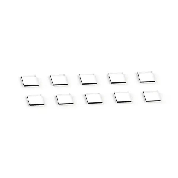
Single Crystal CVD Diamond Plate — undoped, polished surface
Single Crystal CVD Diamond Plate — undoped, polished surface
Historical diamond wafers were limited to small sizes — useless for modern AI packaging. Our advanced CVD technology changes everything.
Standard rectangular plates ship today. Larger wafer-scale formats are available under qualification for selected partners.
Single-crystal diamond delivers the highest thermal conductivity of any material — spreading hotspots evenly across entire substrates.
An epi-ready surface option enables atomic-level direct bonding for GaN-on-Diamond and other advanced heterostructures.
Sign in to see the standard geometries, surface-finish options, and thickness ranges for our SCD plate line. Custom DFM is available for any footprint.
Our SCD plates enable wafer-level packaging, GaN-on-Diamond integration, and extreme-power testing.
2.5D/3D Advanced Packaging for AI accelerators
Contiguous SCD plates spread extreme localized heat (hotspots) from the GPU die evenly across the substrate, preventing thermal throttling and protecting adjacent HBM stacks.
GaN-on-Diamond or Silicon-on-Diamond
The epi-ready surface option allows atomic-level direct bonding for massive arrays of RF or power chips with integrated diamond heat sinks.
Wafer-level testing of 1000W+ HPC chips
Prevents unpackaged semiconductor chips from self-destructing due to overheating during high-current fab testing, dramatically increasing yield rates.
Gallium Nitride (GaN) on Diamond substrates are ideal for CPO laser driver ICs. GaN provides high electron mobility for high-frequency operation, while diamond provides extreme thermal conductivity to handle the heat load from dense laser arrays.
The standard form factor enables standard fab processing for GaN-on-Diamond heteroepitaxy, making it viable for high-volume CPO optical engine production.
Sign in to see the most frequently manufactured SCD configurations across rectangular plates and round wafers. Custom DFM is available for any geometry.
Sign in to see our extended-capability table (including current wafer-scale qualification) and to discuss Custom DFM for non-standard footprints.