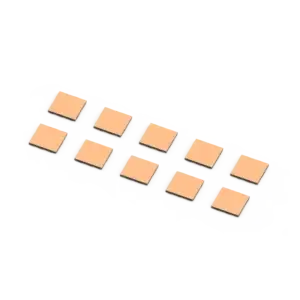
Cu-Metallized Diamond — patterned copper routing on diamond thermal core
Cu-Metallized Diamond — patterned copper routing on diamond thermal core
Copper metallization enables direct die attachment and electrical routing while diamond handles extreme thermal loads.
Round, square, or octagonal baseplates in standard and custom shapes. Custom DFM available for CPO switches, optical engines, and laser submounts.
Custom copper plating and trace routing. NRE required for custom masking. Other metals available for specialized requirements.
Single-crystal diamond base instantly removes junction heat, extending laser lifespan and increasing optical output power limits.
Our Cu-metallized SCD substrates are engineered for extreme-density AI hardware. Custom trace layouts allow direct die attachment while drawing away devastating heat loads.
From CPO switches to laser arrays, our Cu-metallized substrates enable next-generation power delivery and thermal management.
51.2T/102.4T network switch ASICs
Cu-plated SCD baseplates provide identical CTE and sub-0.1K temperature uniformity across the entire switch, maintaining absolute optical alignment while providing electrical routing for drivers.
48V to 1V multi-chip power conversion
Cu-metallization allows direct AuSn soldering of multiple power diodes and MOSFETs onto a single diamond plane. Shrinks footprint by allowing tight component packing without thermal cross-talk.
CW laser arrays for CPO external light sources
Copper traces enable multi-channel electrical driving of dense EML/DML laser arrays while the SCD base instantly removes junction heat, extending laser lifespan and increasing optical output power limits.
Sign in to see the most frequently manufactured Cu-Met configurations, dimensions, and metallization options. Custom DFM is available for any geometry.
Sign in to see the wafer-scale qualification table and Custom DFM options for non-standard footprints.