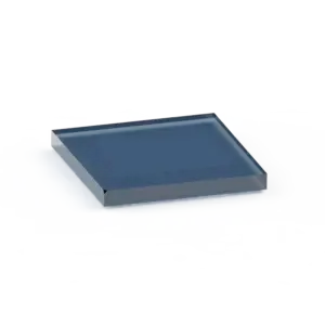
Diamond IC Packaging Lid
Patent-Pending Technology

Integrated Diamond
IC Packaging Lid

All-in-one diamond packaging lid with in-situ temperature sensing, EMI absorption, and electrical insulation. Multi-layer CVD epitaxy for 2.5D/3D packaging and co-packaged optics.

Four Functions. One Diamond Layer.

Replaces bulky multi-component assemblies with a single monolithic diamond structure. Based on our latest multi-layer CVD epitaxy patents.

EMI Absorption

BDD core absorbs microwave interference 1–100 GHz

Electrical Insulation

Intrinsic diamond base (>1E10 Ω·cm) prevents short-circuiting

In-Situ Thermal Sensing

BDD resistance-to-temperature monitoring 25°C–150°C

External EMI Shielding

Optional metal coating (Cu, Ag, Ni, Au) blocks external EMI

Multi-Layer Structure

A Completely Integrated Diamond Structure

Based on our latest multi-layer CVD epitaxy patents, we offer a completely integrated, all-in-one packaging lid for sensitive, ultra-high-density integrated circuits.

This composite diamond structure provides simultaneous bare-die electrical insulation, microwave absorption, external EMI shielding, and—most uniquely—in-situ temperature sensing using the temperature-dependent resistance of our Boron-Doped Diamond layer.

The result: real-time, highly localized junction temperature readings directly above the IC, allowing system logic to adjust cooling instantly without latency from external sensors.

Composite Diamond Structure

Top/Outer Layer 30–100 µm

Optional metal coating (Cu, Ag, Ni, Au)

Core Layer BDD

Microwave absorbing + heat spreading + thermal sensing

Base Layer (Die-facing) 10–50 µm

Intrinsic Diamond: >1E10 Ω·cm electrical insulator

Sidewalls OFC (Oxygen-Free Copper) or Al Alloy

Hermetic/semi-hermetic sealing

In-Situ Thermal Sensing Range: 25°C – 150°C
Common Form Factors

Dimensions for Advanced Packaging

Our patent-pending composite diamond lids are frequently adapted to the following high-density applications. We also offer Custom DFM for exact footprints.

Dimensions (mm) Structure Target Applications
8 × 8 to 15 × 15 Submounts with integrated sidewalls OSFP and QSFP-DD transceiver modules, dense EML/VCSEL laser arrays
15 × 15 to 30 × 30 Full lid with customizable sidewall height Co-Packaged Optics (CPO) - Optical Engines (PIC + EIC chiplets)
30 × 30 to 60 × 60 Large-area MCM lid with intrinsic diamond base Advanced 2.5D/3D System-in-Package (SiP) covering multiple bare dies

Optional: Integrated Micro-Channels & Heat Fins

For enhanced fluid or air cooling, we offer CVD-grown or laser-etched micro-channels and heat fins with 50–500 µm height/depth precision.

50–500 µm height/depth CVD-grown or laser-etched

Matched Parts & Applications

Engineered for the most demanding ultra-high-density integrated circuit packaging applications.

Bare-Die Multi-Chip Modules (MCM)

System-in-Package (SiP) designs

The 10–50 µm intrinsic diamond layer prevents electrical short-circuiting against bare dies, allowing the heat spreader to be placed in direct, intimate contact with silicon. This maximizes heat transfer while the BDD core absorbs inter-chip microwave interference.

Co-Packaged Optics (CPO) & Photonic ICs

Thermal management for laser arrays

Lasers are highly sensitive to temperature drift. The lid's built-in temperature sensing provides real-time, highly localized junction temperature readings directly above the PIC, allowing system logic to adjust cooling instantly without latency from external sensors.

6C Standard Sizes

8×16 to 10×80mm (PIC to MCM)

Need a Custom Configuration?

We manufacture custom DFM (Design for Manufacturing) for exact footprints, layer stacks, and thermal sensing requirements. Contact us with your specifications.