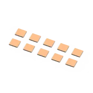
EMI-Absorbing BDD Heat Spreader — diamond thermal core with Cu metallization
EMI-Absorbing BDD Heat Spreader — diamond thermal core with Cu metallization
Standard metal lids reflect EMI, causing devastating internal crosstalk. Our BDD substrate absorbs electromagnetic energy and instantly converts it to heat.
Unlike metal lids that bounce high-frequency signals back onto the die, our BDD lid absorbs stray EMI and prevents cavity resonance.
1000–2000 W/m·K thermal conductivity draws massive heat loads away from the silicon junction without electrical conduction.
Sign in to see the full attenuation tuning range, low/high attenuation trade-offs, and recipe details for matching your specific EMI absorption target.
Ordinary pure diamond is an electrical insulator and is completely transparent to microwaves, offering zero EMI attenuation. To solve extreme thermal and signal integrity challenges in next-generation AI data centers, we engineered a diamond plate that acts as a tunable microwave absorber.
By engineering our proprietary diamond material, we created a diamond plate that absorbs electromagnetic energy in the 1 GHz to 100 GHz range and instantly converts it to heat—all while acting as an ultra-high thermal conductivity heatsink.
Sign in to see the full dimension and thickness table for AI GPU lids, SerDes packaging, and mmWave ASICs. Custom DFM is available for any footprint.
Sign in to see our extended-capability table (including current 100mm wafer-scale qualification) and to discuss Custom DFM for non-standard footprints.
Engineered for the most demanding high-frequency, high-power applications in AI and communications infrastructure.
Direct-to-die lids for 1000W+ AI accelerators
Standard metal lids bounce high-frequency signals back onto the die. Our BDD lid absorbs stray EMI, preventing cavity resonance and internal crosstalk, while drawing massive heat loads away from the silicon junction.
PCIe Gen 5/6 & NVLink SerDes and retimer chips
Absorbs signal noise in the critical 1–100 GHz band, ensuring maximum data throughput and signal integrity without sacrificing the thermal budget required by high-speed switching.
Telecommunication basestation chip packaging
Replaces bulky multi-component assemblies (separate heat sinks + microwave absorbers) with a single monolithic diamond layer, dramatically shrinking the module footprint.
BDD heat spreaders provide EMI absorption and thermal spreading for CPO optical engines. The PIC (Photonic Integrated Circuit) and EIC (Electronic IC) chiplets generate both heat and high-frequency noise that BDD handles simultaneously.
Silicon Photonics Thermal Management
Individual BDD lids for PIC chiplets absorb 1-100 GHz microwave interference from dense optical modulators while spreading heat from laser diodes.
CMOS Driver/TIA Circuitry
EIC chiplets (CMOS drivers, TIAs) operate at high frequencies with switching noise. BDD absorption prevents cross-talk between dense electronic and photonic circuits.
Multi-Chip Module Integration
Full MCM modules combining PIC + EIC + support dies require large-area BDD lids for thermal spreading across the complete optical engine assembly.
Sign in to see the standard sizes we offer for PIC chiplet lids, EIC chiplet lids, and MCM thermal lids.
The BDD heat spreader is one application of our boron-doped diamond technology. We also produce PCD-based BDD electrodes on standard substrates, and copper-plated thermal spreaders.
Boron-doped polycrystalline diamond film on Si substrate for electrochemistry and water treatment.
PCD CoatingBDD on Nb for high-temperature electrochemical sensors and superconducting RF applications.
PCD CoatingBDD on Ti for biomedical implants and corrosion-resistant electrochemical cells.
PCD CoatingPolycrystalline diamond film on glass for Through-Glass Via (TGV) interposer applications.